The Vinod Dham Centre of Excellence for Semiconductors and Microelectronics has been inaugurated in Delhi, marking a significant step in developing India’s semiconductor talent.

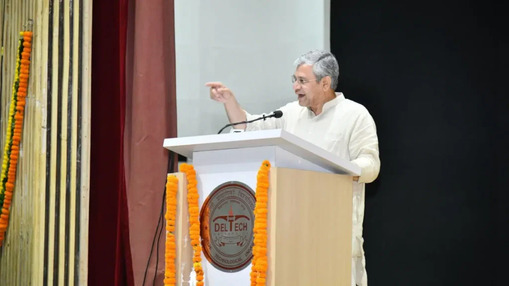
Union electronics and IT minister Ashwini Vaishnaw, along with Vinod Dham, known as the ‘Father of the Pentium Chip’, inaugurated the new building at Delhi Technological University (DTU) on Monday.
The centre will support research, development, and talent training efforts nationwide. It will serve students, institutions, and industry partners working on semiconductor design and microelectronics.

The initiative is part of the government-backed Chips to Startup (C2S) programme. Over one lakh B.Tech, M.Tech, and PhD students have been onboarded under the scheme.
“263 institutions have been supported with world-class Electronic Design Automation (EDA) tools,” Vaishnaw mentioned in a post on X.
He also mentioned that the programme has enabled 65 R&D projects across 113 organisations, alongside a dedicated SMART lab established at NIELIT, Calicut. Moreover, the ChipIN Centre has conducted 170 training sessions so far.
As part of the design and fabrication outcomes, 20 Application-Specific Integrated Circuits (ASICs) have been fabricated at the Semi-Conductor Laboratory (SCL) foundry, and 14 ASICs have been sent for fabrication.
Rishu Chaujar, the centre’s director, outlined plans for future phases, including collaborations with international universities and industry partners. It is expected to play a key role in reducing India’s dependence on imported chips and strengthening domestic capability. It aims to drive innovation and knowledge creation in semiconductors and microelectronics, aligning with the India Semiconductor Mission (ISM).

Dham praised India’s ISM, which he believes will open new opportunities for the country. He emphasised the importance of institutions working together to achieve national goals like Atmanirbhar Bharat. Vaishnaw also encouraged students to seize opportunities and contribute to India’s semiconductor journey.
The C2S program is part of a larger push by the Indian government and aims to train specialised manpower in Very-Large-Scale Integration (VLSI) and Embedded System Design (ESD).
As India moves towards launching its first homegrown semiconductor chip, these developments are pivotal in reducing dependency on imports and fostering self-reliance in advanced technology.
📣 Get ready for the AI event of the year—sign up for Cypher today!